SuperFlash® Memory Technology
Why Choose SuperFlash® Memory?
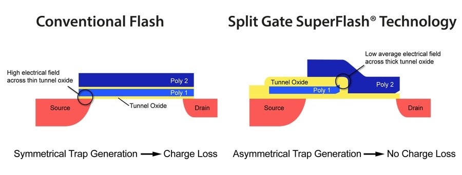
High Reliability and Data Retention
SuperFlash technology utilizes a much thicker oxide layer than traditional stacked-gate Flash. The thicker oxide layer is much less susceptible to defects and damage that can create a leakage path and eventual cell data loss. Notice that the floating gate of the SuperFlash technology cell also has a hook or notch at the edge. This hook creates a strong electric field that improves the performance and reliability of erase operations.
Industry's Fastest Erase Times
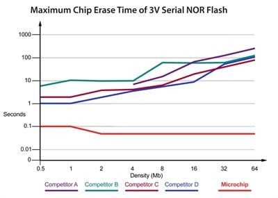
The unique split-gate cell design allows products with SuperFlash technology to provide the fastest sector, block and chip erase times available. While a typical 64 Mb Flash can take as long as 100 seconds to perform a full chip erase, the equivalent products with SuperFlash technology can complete the same operation in less than 100 ms.
As shown in Figure1, chip erase times become more significant as the density increases in competing devices. With SuperFlash technology, the chip erase remains extremely fast regardless of density.
Over-erase is a condition that affects traditional stacked gate Flash. An over-erased cell creates a leakage current path between the drain and floating gate, which can result in read failures. To combat this effect, stacked gate Flash requires multiple erase pulses, soft-programming and erase verification cycles to ensure a tight threshold voltage window of the Flash cell. Over-erase and the resulting cell leakage does not affect the split gate cell design of SuperFlash technology because the floating gate is isolated from the drain. Therefore, the additional soft-program and erase verify steps during cell erase are not required with SuperFlash technology. The result is a Flash memory that can perform a full chip erase up to 1,000 times faster than typical Flash.
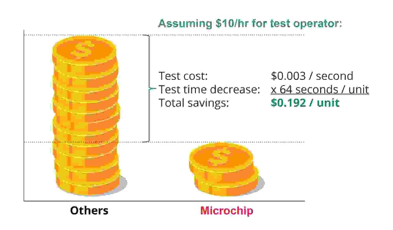
Faster Erase Times Save You Money
Your factories may be wasting valuable time testing Flash memory. SuperFlash memory drastically improves manufacturing throughput, saving test costs and avoiding the investment in additional test equipment to meet your customers’ demand. Stacked gate Flash requires minutes per board whereas SuperFlash only needs seconds. Don’t get caught off guard by this hidden product cost.
We have created an interactive savings calculator to show you what your annual savings might be if you choose SuperFlash technology. Give it a try.
Learn More About the Advantages of SuperFlash® Technology
This video provides a technical overview of the key advantages that SuperFlash memory offers over conventional NOR Flash memory. It compares the functions of the memory cells of both to demonstrate how SuperFlash memory offers better endurance, lower power consumption and 1000 times better erase times.
Are You Ready to Use SuperFlash Technology?
Now that you know about how using SuperFlash Technology can save both time and money, find the right SuperFlash memory device for your application. We provide key design considerations to make product selection easy.