We detect you are using an unsupported browser. For the best experience, please visit the site using Chrome, Firefox, Safari, or Edge. X
Maximize Your Experience: Reap the Personalized Advantages by Completing Your Profile to Its Fullest. Update Here
Stay in the loop with the latest from Microchip. Update your profile while you are at it. Update Here
Complete your profile to access more resources. Update Here

Getting Started With SuperFlash® Technology

How to Find the Best NOR Flash Solution for Your Design
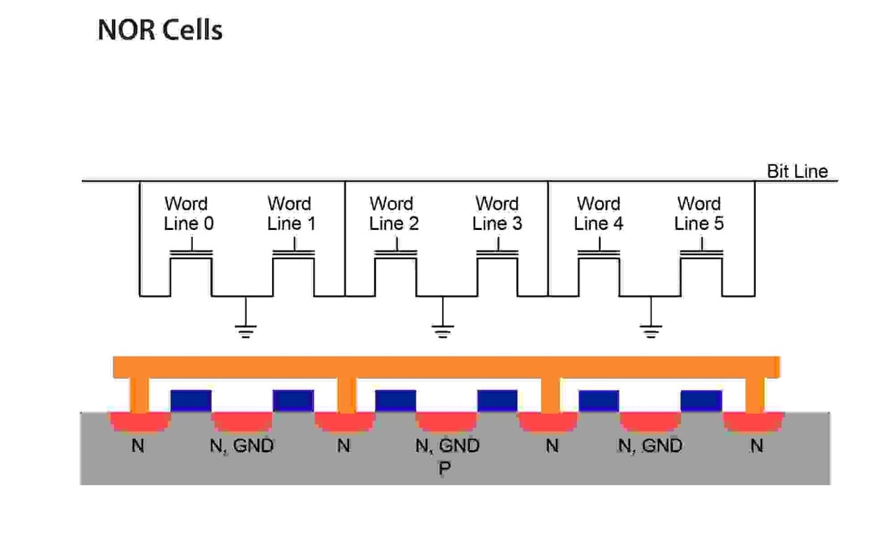
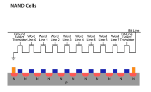

We offer a wide range of NOR Flash products in a variety of bus interfaces, speeds, voltages and packages. Here is some information that you should consider when selecting a Flash solution for your design.

NOR vs. NAND Flash


NOR and NAND Flash differ in the way connections are made between the individual memory cells. In NOR Flash, each cell is individually connected to the bit line in parallel. NAND Flash cells are connected in series to a bit line. The series connection reduces the number of ground wires and bit lines, resulting in a higher-density layout. For a given process technology and density, a NAND Flash memory is about 60% smaller than a NOR Flash memory. This provides a lower cost per bit than NOR Flash. However, NAND Flash does not provide a random-access external address bus. Therefore, data can only be read in pages. This makes NAND Flash similar to data storage devices like hard disk drives and optical memory. On the other hand, NOR Flash is better suited for accessing program code such as a computer’s BIOS or firmware. NOR Flash memory is read similarly to random-access memory, which is excellent for execute-in-place applications.


  NAND NOR
Main Application File Storage Code Execution
Storage Capacity High Low
XIP Capabilities No Yes
Cost per Bit Better  
Active Power Better  
Standby Power   Better
Write Speed Good  
Read Speed   Good

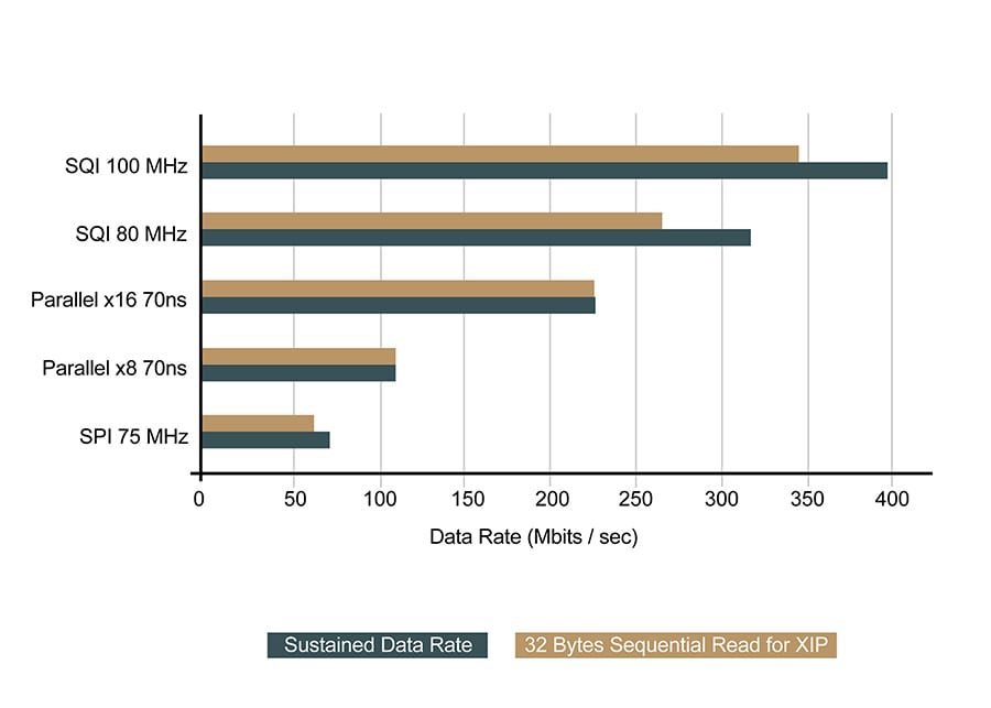
Parallel vs. Serial SPI vs. Serial SQI™ Flash Devices


NOR Flash is available with either a serial or parallel bus interface. The choice of which bus to use is often dictated by the required data rates of the application as well as the amount of available I/O on the microcontroller and the board space available. With the ongoing demand for smaller and cheaper products, more designs are now being switched to a serial interface to reduce board space and component price.

Today’s microcontrollers are often bond pad-limited. This means that the size of the die is limited by the space needed for bond pads rather than for the microcontroller gates/circuitry. Eliminating bond pads results in a smaller die, increasing the amount of die on a wafer and resulting in reduced cost per die. Additionally, more pins increase the assembly and packaging costs of both the microcontroller and the memory. This is why there has been a major shift from using parallel Flash to using serial Flash. However, switching to fewer pins means lower data throughput. In order to offset this, a quad I/O serial interface is being used in the latest serial devices to create SQI Flash devices.

  Parallel Serial SPI
Data Throughput High Medium
Pin Count 32+ 8+
Package Size Large Small
Power Consumption Medium Low
Cost High Low

What Is the Common Flash Memory Interface (CFI)?


The Common Flash Memory Interface (CFI) is an open standard approved by JEDEC. The goal of the standard is to allow interchangeability between Flash memory devices from different manufacturers of parallel Flash products. Each manufacturer’s memory has differences in performance specifications, memory maps and features. The standard allows for this identifying information to be read out of a table of values that is stored on the Flash device. The benefit of using this standard is that information about multiple Flash parts no longer needs to be stored in system software. This helps to future-proof the software and allows developers to use lower-cost Flash devices as they become available without needing to update their software.

What is Execution In Place (XIP)?


Execution In Place (XIP) refers to executing program code directly from external storage rather than copying it into RAM first. Running program code from external storage allows additional RAM to be freed up for dynamic data. For XIP to be possible, you must have random access capability, the appropriate memory mapping and sufficient bandwidth. NOR Flash is well suited for execution in place whereas NAND Flash is not. Program code in NAND Flash must be copied into RAM before being executed.

What Is the Serial Flash Discoverable Parameter (SFDP)?


The Serial Flash Discoverable Parameter (SFDP) standard is similar to the CFI standard for parallel Flash. The goal of this JEDEC-approved standard is to allow interchangeability between Flash memory devices from different manufacturers. Each manufacturer’s memory has differences in performance specifications, memory maps and features. The standard allows the use of a single driver that reads identifying information out of a table of values stored on the Flash device. The benefit of using this standard is that information about multiple Flash parts no longer needs to be stored in system software. This helps to future-proof the software and allows developers to use lower-cost Flash devices as they become available without needing to update their software.

Documentation


Brochures

Memory Products Brochure
SuperFlash® Memory Products

Live Chat

Need Help?

Privacy Policy