Overview
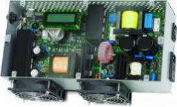
Microchip’s Digital Pure Sine Wave Uninterruptible Power Supply (UPS) Reference Design is based on the dsPIC33F “GS” series of digital-power Digital Signal Controllers (DSCs). This reference design demonstrates how digital-power techniques when applied to UPS applications enable easy modifications through software, the use of smaller magnetics, intelligent battery charging, higher efficiency, compact designs, reduction in audible and electrical noise via a purer sine-wave output, USB communication and low-cost overall bill-of-materials. This reference design is Royalty Free. Click here for a list of complete documentation and software & hardware design information.
This reference design is implemented using a single dsPIC33F “GS” digital-power DSCs from Microchip that provides the full digital control of the power conversion and system management functions. As shown in this reference design the dsPIC33F ‘GS’ devices enable designers to easily and cost effectively create products using advanced switching techniques such as LLC that lower switching losses and enable efficiencies as high as 95%. The DC to DC LLC Converter Reference Design is royalty free when used in accordance with the licensing agreement.
The Digital Pure Sine Wave UPS System operates in two modes:
- Standby Mode – Operational in the presence of AC line voltage; battery is charged in this mode.
- UPS Mode – Operational during power outage; the system switches to a function called inverter to provide power to load. Charge stored in the battery is converted to AC output.
For additional details, demo requests, and design files please visit the reference design page.
- High-frequency design
- Adjustable Charging current
- Efficiency of 84%
- Pure sine wave output with THD <3%
- Mains to Battery Transfer time < 12 ms
- Supports Crest Factor of 3:1
- Minimum Power Factor(Leading/Lagging) of 0.65
- Fault indications
- USB Communication with PC
- LCD front panel
- Digital Pure Sine Wave UPS unit
- Documentation CD consisting of:
- Digital Pure Sine Wave UPS Reference Design Software (220V or 110V version)
- Digital Pure Sine Wave UPS Schematics and PCB Layout files
- Digital Pure Sine Wave UPS MATLAB™ Model Files
- Digital Pure Sine Wave UPS Reference Design User Guide
- Cable Assembly

Documentation
|
Title
|
Document Category
|
|||
|---|---|---|---|---|
| Offline UPS Reference Design Using the dsPIC DSC | Application Notes | Link | Download | |
| Offline UPS Source Code | Supporting Collateral | Download | ||
| Offline UPS Design Package | Supporting Collateral | Download | ||
| Features, Value and Benefits of Digital Control for Power Supplies | Supporting Collateral | Download | ||
| Offline UPS Reference Design Using the dsPIC DSC | Application Notes | Link | Download | |
| Frequently Asked Questions (FAQs) About dsPIC® DSC SMPS Devices | FAQ | Download |