Overview
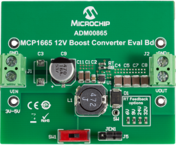
The MCP1665 12V output boost regulator evaluation board is intended to provide a platform allowing customers to easily evaluate the features of the MCP1665 device in a typical boost toplogy while also providing a reference for proper choice and layout of components that are critical to switching regulator implementations.
The MCP1665 12V Output Boost Regulator Evaluation Board has the following features:
· Typical 12V Output when supplied from a low-input voltage source
· Input Voltage range (VIN): 3V to 5V, with VIN < VOUT
· Output Current: max 1 A @ 12V Output with 5V Input
· Enabled state is selectable by using EN jumper
· Light-load power saving method is selectable by toggling the MODE switch
· Undervoltage Lockout (UVLO)
o UVLO Start: 2.9V
o UVLO Stop: 2.7V
· PWM/PFM Operation
· PWM Switching Frequency: 500 kHz
· Peak Input Current Limit of 3.6A (typical)
· Internal Compensation, so no compensation network is needed on the board
· Soft Start
· Protection in case of feedback pin shorted to GND
· Overtemperature Protection (if the die temperature exceeds +150°C, with 15°C hysteresis)
1x MCP1665 12V Boost Converter Eval Bd (ADM00865)
Documentation
|
Title
|
Document Category
|
|||
|---|---|---|---|---|
| MCP1665 12V Output Boost Regulator Evaluation Board User's Guide | User Guide | Download | ||
| MCP1665 High-Voltage 3.6A Integrated Switch PFM/PWM Boost Regulator | Data Sheets | Download | ||
| MCP1665 12V Boost Converter Eval Bd (ADM00865) Gerbers | Board Design Files | Download | ||
| MCP1665 12V Boost Converter Eval Bd (ADM00865) BOM | Board Design Files | Download | ||
| MCP1665 12V Boost Converter Eval Bd (ADM00865) Schematic | Board Design Files | Download |