Log in to myMicrochip to access tools and benefits. Sign up in just one minute.
Maximize Your Experience: Reap the Personalized Advantages by Completing Your Profile to Its Fullest. Update Here
Stay in the loop with the latest from Microchip. Update your profile while you are at it. Update Here
Complete your profile to access more resources. Update Here
Overview
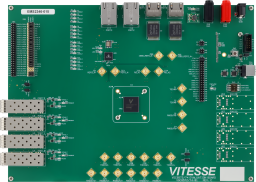
The VSC8574 evaluation board provides the user a way to evaluate the VSC8574 device in multiple configurations. Four RJ-45 connectors are provided for copper media interfaces. The four SFP cages allow for evaluation of the fiber media interconnects. The MAC interface is provided via SMA connectors or alternatively through SFP ports.
For access to all of the features of the device, an external microcontroller is used to configure the onboard clock chip via a two wire serial bus and the VSC8574 via the MDIO bus. The graphical user interface (GUI) enables the user to access the registers.
The evaluation board uses a Zarlink device to synthesize a 125MHz reference clock signal from a 20MHz crystal which serves as the REFCLK input.

Cannot load image!
Documentation
Filter by Document Type
Search Documentation
|
Title
|
Document Category
|
|||
|---|---|---|---|---|
| VSC8574 Evaluation Board User Guide | User Guide | Download | ||
| VSC8574EV Evaluation Board Schematic | Board Design Files | Download | ||
| VSC8572EV BOM | BOM | Download | ||
| VSC8572-74 Assembly Files | Board Design Files | Download | ||
| VSC8572-74 Fabrication Files | Board Design Files | Download |