Versatile, Compact and High-Performance TySOM-M Embedded Development Board Based on PolarFire® SoC FPGA Device
Learn more about Aldec's high-performance and versatile FPGA development platform.

High-Performance FPGA Development Platform With Hardened RISC-V Cores
With the increasing adoption of RISC-V cores into a wide range of applications that require low power and high security, having a high-performance and versatile Field-Programmable Gate Array (FPGA) development platform with hardened RISC-V cores is highly critical. Aldec, an Electronic Design Automation (EDA) pioneer and a member of the Mi-V ecosystem, has developed and produced TySOM-M, a Linux®-capable, multi-core, RISC-V-based platform featuring the PolarFire® System-on-Chip (SoC) FPGA MPFS250T-FCG1152 device. The board includes multiple peripherals with dual FPGA Mezzanine Card (FMC) connectivity to support various applications without having to develop custom hardware.
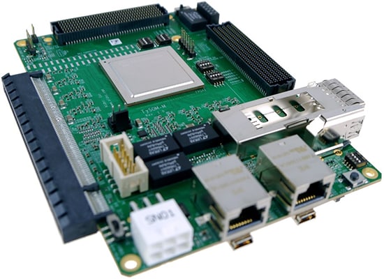
This compact board (144 mm × 100 mm) is well suited for the development/prototyping of secure and power-efficient designs targeting Software Defined Radio (SDR), Machine Learning (ML), Internet of Things (IoT), industrial automation, automotive, aerospace and defense, wireless access networks and cellular infrastructure.
The Board Support Package (BSP) includes reference designs, a Microprocessor Subsystem (MSS) configuration, a Hart Software Services (HSS) configuration, an Aldec meta layer for Yocto Project and a bare metal application—all of which can be used to build a custom design.
Chipset/SoC:
Memory
|
Interfaces
|
For versatility, Aldec provides a comprehensive list of FMC daughter cards that can be used with TySOM-M to enable various types of I/O interfaces. As a few examples:
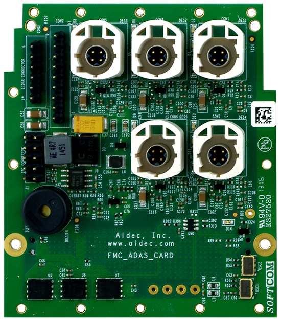
FMC-ADAS Daughter Card
The FMC-ADAS daughter card enables prototyping and evaluation of automotive and Advanced Driver Assistance System (ADAS) designs with TySOM. It extends the base functionality of a given FPGA board by providing interfaces and peripherals for HSD cameras, RADAR, LIDAR and ultrasonic sensors that are the base of ADAS applications. For example, 360° car vision or rear-view camera applications and supporting algorithms can be evaluated with HSD cameras attached directly to the FPD-Link III Deserializer (Texas Instruments DS90UB914Q-Q1) on the FMC-ADAS card.
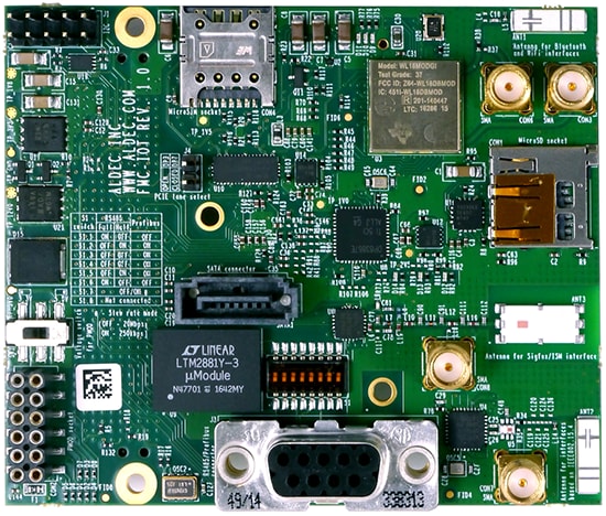
FMC-IOT Daughter Card
The FMC-IOT daughter card provides a set of peripherals and interfaces commonly used in embedded designs for IoT applications. There are various wireless communication standards used in such designs and this board enables prototyping with any of the Wi-Fi®, Bluetooth®, ZigBee, Sub-GHz RF devices and wired Ethernet and USB.
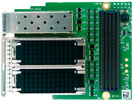
FMC-QSFP Daughter Card
The FMC-QSFP daughter card provides QSFP+ and SFP+ extension of FPGA prototyping boards with standard FMC connectors. It can be used in networking applications that require high bandwidth connection to external environments such as implementation of low latency high bandwidth links used in High Performance Computing (HPC) or High Frequency Trading (HFT). It supports 27.8125 Gb/s per each channel in QSFP+, which amounts to 100+ Gb/s on each QSFP+ connector depending on the main device.
FMC-INDUSTRIAL Daughter Card
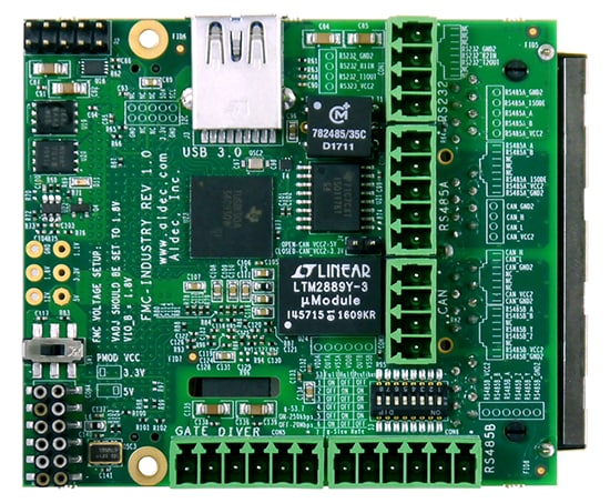
The FMC-INDUSTRIAL daughter card enables prototyping and evaluation of industrial applications that require standard serial communication interfaces with versions improved for QoS and immunity to rugged conditions. The board contains isolated versions of RS485 and RS232 that are well established in various industries. Additionally, there is a CAN controller that also provides an isolated physical interface that is widely used in automotive applications. Except for the hardened serial interfaces, industrial applications very often exploit standard computer interfaces, hence why this board provides the USB 3.0. It can be further expanded with the Digilent PMOD modules.
FMC-PCIe Expansion Daughter Card
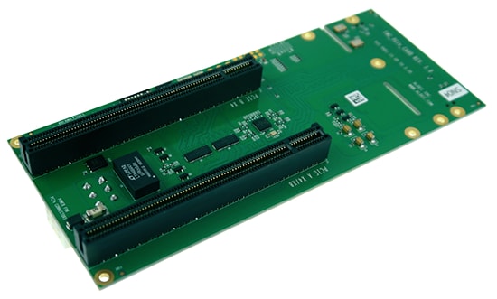
The FMC-PCIe expansion daughter card can be used as PCIe root complex and provides two PCIe ×4 interfaces or one PCIe ×8 interface for endpoint cards equipped with standard PCIe finger connectors up to ×16. This board includes two PCIe connectors on the bottom. There are four PCIe lines which can be switched between two PCIe connectors using passive switches on the board. The 100 MHz reference clocks for PCIe and FMC connectors are generated using Low Voltage Differential Signaling (LVDS) oscillators on the card.
Choosing an FPGA development board for a given project is not as easy as it sounds. It requires meticulous planning beforehand. One of the worst-case scenarios that can happen is needing a new I/O interface due to a requirement change after the final system prototype has already been validated, but the new I/O interface is not supported by the current FPGA board. Sourcing a new FPGA board would entail migrating the entire system design to a new chipset. Verification, implementation and validation can of course be rerun, but unexpected issues and bugs will most likely arise. To avoid these sort of potential project issues, versatility is key and must be carefully taken into consideration.
Aldec has been a long-term partner of our FPGA business unit for over 35 years. Aldec is an EDA pioneer and a member of the Mi-V ecosystem. Aldec provides advanced verification solutions needed for mid- to high-density FPGAs and SoC FPGAs, including mixed-Hardware Description Language (HDL) simulation, code coverage, functional coverage, assertions-based coverage, constrained-random simulation, static linting, Clock Domain Crossing (CDC) analysis and FPGA development boards.
For a complete list of Aldec's FMC daughter cards, please visit their website. To learn more about their offerings, please contact them.