
Taking Custom Logic Further With the Latest CLB Enhancements
A brief look at the CLB peripheral on the new PIC18F-Q35 microcontroller and how it expands on the CLB from its previous iteration.

Introducing the CLB
With the release of the PIC16F13145 microcontroller (MCU), Microchip introduced the Configurable Logic Block (CLB) peripheral, enabling programmable logic within the MCU. The purpose of the CLB was to give embedded designers a way to implement simple programmable logic directly on the MCU, no external CPLD or FPGA required. The CLB provides easily configurable, hardware-based logic for designs at a fraction of the cost of competing solutions. Since its introduction, the CLB has been refined and expanded in subsequent devices, the PIC16F132 family and PIC18-Q35 family of MCUs. For those already familiar with the first iteration of the CLB, much of its design will remain familiar. The implementation of these new devices represents a meaningful architectural step forward and this article walks through what changed and why it matters.
More Logic, More Possibilities…
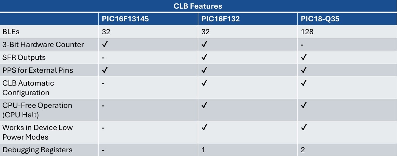
The core building block behind the CLB is its Basic Logic Elements (BLE). Each BLE is a four input LUT (Lookup Table) and acts as its own logic element that can be customized to respond with a variety of digital functions. The biggest obstacle to large or complicated digital designs on the CLB is running out of these BLEs. The PIC16F132 family contains 32 BLEs and a built-in 3-bit counter, just like the original PIC16F13145 family. The PIC18F-Q35 family CLB does not contain the built-in 3-bit counter, but has been expanded to 128 BLEs, four times as many as the original.
To aid with monitoring and debugging these BLEs, the CLB on both the PIC16F132 and PIC18F-Q35 families now include Special Function Registers (SFR) outputs to easily read up to 16 BLE outputs.
Connections Are Everything, so We Expanded Them…
The PIC18F-Q35 family of microcontrollers also broadens how the CLB interacts with the rest of the device. The peripheral connections for the CLB have been expanded to include the Pulse Width Modulator (PWM), Complementary Waveform Generator (CWG) and Digital Signal Modulator (DSM) peripherals for improved Waveform Control giving more options for motor control applications and digital signal processing. Additionally, the PIC18F-Q35 family CLB includes connections to the Device SRPORT for further peripheral connections without using up valuable external Device I/O pins. For real-time control-based applications, where moving data quickly across the device is critical, the PIC18F-Q35 CLB is also compatible with the on-board DMA peripheral for fast data transfers independent of the CPU.
While these connections are specific to the PIC18F-Q35 family, the CLB Peripheral Pin Select (PPS) outputs from the original CLB still remain for both new families for direct connections to external device pins.
Your Configuration When You Need It…
Both new families’ CLB peripherals have new options for running independently from the CPU. For faster start times, the CLB Automatic Configuration allows the CLB to be immediately configured on device start-up. Complementing this capability, both device families also support a CPU halt mode, enabling the CLB to continue to operate along with other peripherals while the CPU is stopped. For low-power applications like IoT or battery-operated devices, the CLB can also operate in device low-power modes, provided the configured logic is asynchronous, or the required oscillator is active. This allows the CLB to maintain its functionality while other parts of the device like your CPU focus on conserving power.
Easier Debugging, for Fewer Design Headaches…
To assist development on the latest iteration of the CLB, additional capabilities have been introduced. The PIC16F132 CLB includes one debugging register while the PIC18F-Q35 CLB includes two. These registers allow developers to easily select the output of specific BLEs to either read internally (similar to the SFR output) or route externally using Peripheral Pin Select (PPS). This provides a straightforward way to validate your logic design during the development.
On the software side, the CLB Synthesizer has been upgraded for all CLB equipped devices. It now supports design simulation prior to programming your device for faster iterations and easier debugging. Furthermore, the CLB Synthesizer can provide timing analysis to report maximum CLB clock speed while delivering functional behavior, helping you maximize your design’s performance.
To Wrap Things Up…
In short, the latest CLB implementations in both product families build on the original concept with significant improvements, including expanded logic capacity; improved visibility with software-readable outputs and dedicated debug registers; and broadened system integration through PPS outputs, peripheral connections, DMA compatibility, automatic start-up configuration and operation in Sleep mode under supported conditions. Together, these enhancements make the newer CLB a more capable and practical solution for adding flexible hardware-based logic to embedded designs without the cost and PCB space of larger programmable logic devices.