The Fundamentals of Linear Voltage Regulators With Low Dropout (LDO)
What Are Linear Regulators?
Linear regulators are a simple solution for using an integrated circuit to regulate a higher voltage to a lower voltage without the use of an inductor. Linear regulators span a wide spectrum of specialized uses and can be widely implemented in today’s electronics because of their simplicity and low cost.
What Does Low Dropout (LDO) Mean?
Dropout voltage is the minimum voltage difference required between the input voltage and desired output voltage for the linear regulator to provide sufficient regulation. If the voltage difference between input and output is lower than the specified dropout voltage, the linear regulator will enter dropout mode, where the device ceases to regulate the input voltage and the output voltage will track the input voltage. Linear regulators with lower dropout voltage have the advantage of regulating input voltages with smaller margins to the desired output voltage. In other words, the lower the specified dropout voltage, the closer the input voltage can be to the output voltage while maintaining regulation.
How Do Linear Regulators Work?
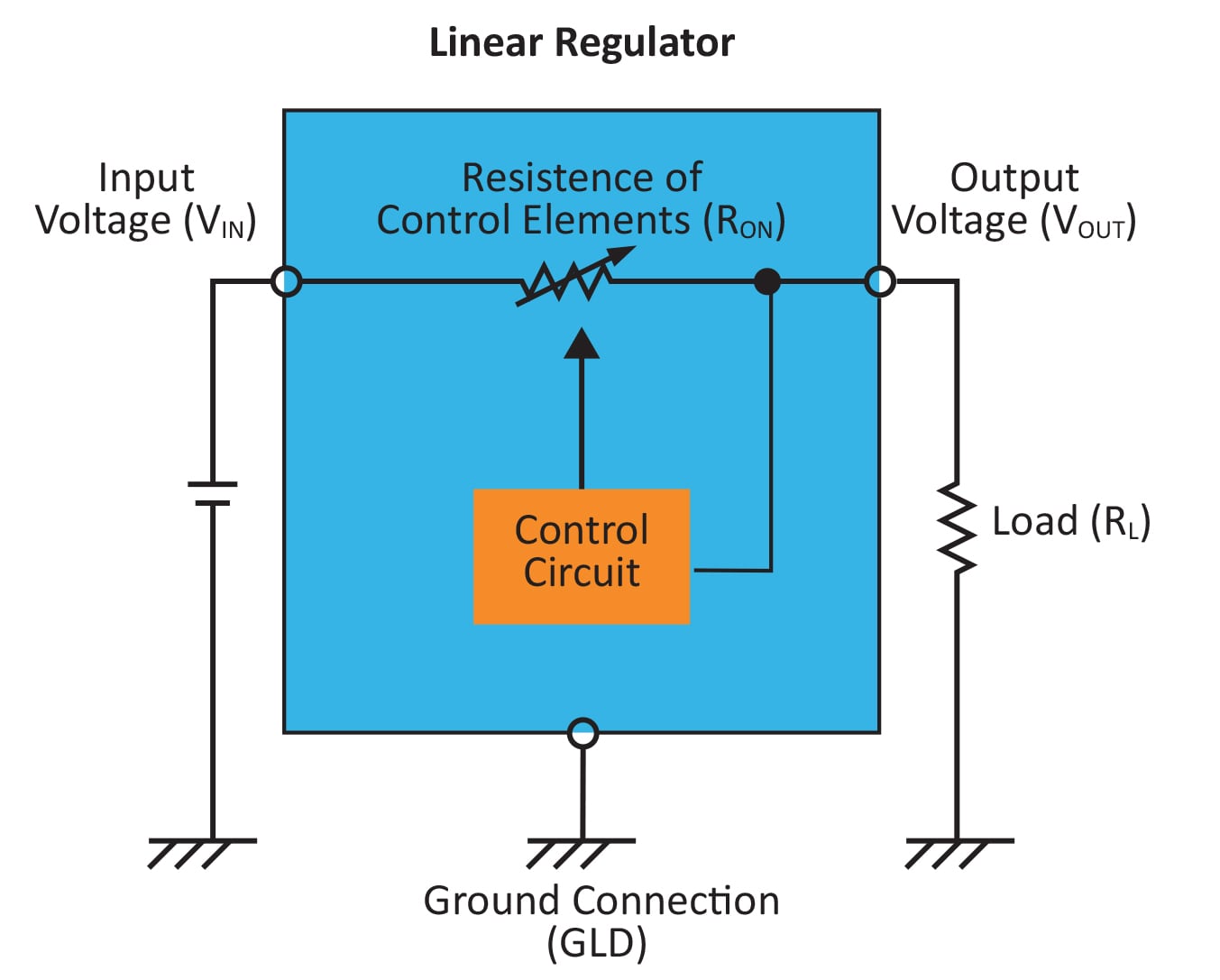
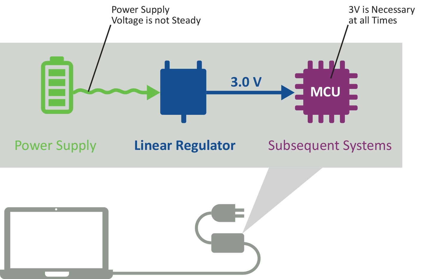
In simple terms, an LDO linear regulator regulates the input voltage from a source, like a battery, into a lower output voltage that can be used by a device on the load side, commonly a microcontroller (MCU).
There are two major LDO architectures, PMOS and NMOS, that achieve voltage regulation. Regardless of architecture, LDOs achieve voltage regulation via a feedback loop that allows the circuit to control the drain-to-source resistance. The difference between PMOS and NMOS can be summarized in how the error amplifier relates to the gate-to-source voltage. In a PMOS architecture, as Vin approaches Vout, the gate-to-source voltage is driven negative to lower the drain to source resistance and provide voltage regulation. In an NMOS architecture, the error amplifier drives gate-to-source voltage more positive to decrease the drain-to-source resistance as the input voltage approaches the output voltage. The NMOS architecture encounters a roadblock to achieving LDO because the gate-to-source voltage begins to drop once the error amplifier saturates as VIN approaches VOUT. Therefore, it is common for a NMOS LDO to implement either a bias voltage rail or a charge pump to achieve LDO performance.
Outside of the architecture, other variables contribute to the LDO performance such as output current, junction temperature and accuracy.
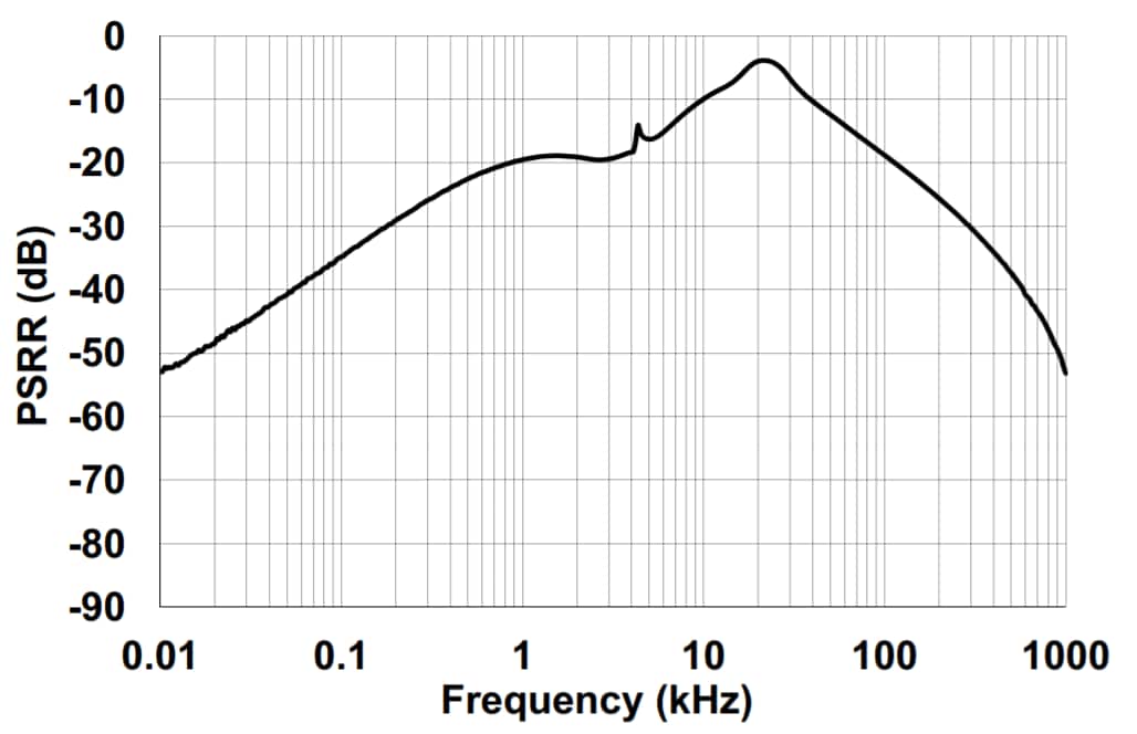
What Is High PSRR?
In the process of dropping input voltage to output voltage, various unwanted frequencies could find their way into the integrated circuit. The Power Supply Rejection Ratio (PSRR) of a linear regulator is the measurement of how well the integrated circuit filters and rejects extraneous noise in the input voltage signal before voltage is outputted. High PSRR typically correlates to a more consistent output accuracy.
How to Choose an LDO Regulator
- Low Dropout
- Accuracy
- PSRR
- Low Quiescent Current
Low Dropout
Although there are many ways to utilize an LDO regulator, maintaining a low dropout between the input and output voltage is the LDO regulator’s primary purpose. This is an important aspect to consider before choosing an LDO regulator as a power regulation solution.

Accuracy
As the performance and capability of technology continues to grow at a rapid rate, it is crucial that the core components of these devices meet stringent requirements and operate on a consistent and leading-edge basis. The LDO regulator’s responsibility is not only to have a low input-to-output dropout but also to ensure that the voltage is outputted with the smallest margin of error.

PSRR
In the process of dropping input voltage to output voltage, various unwanted frequencies could find their way into the integrated circuit. The PSRR of a linear regulator is the measurement of how well the integrated circuit filters/rejects out extraneous noise in the input voltage signal before voltage is outputted. High PSRR typically correlates to a more consistent output accuracy.
Low Quiescent Current
Also known as Iq, quiescent current is the current that is drawn from an integrated circuit while it is in a quiescent (no-load, non-switching) state. IQ can be understood as the minimal amount of current needed to power the basic functionalities of a device. The lower the rated quiescent current of a linear regulator, the more power efficient the linear regulator is in a no-load state.

Featured Products
MCP1722
- AEC-Q100, Grade 0 qualified, PPAP capable
- Low Quiescent Supply Current: 50 μA
- Low Shutdown Quiescent Supply Current: 4 μA
MCP1711
- Low Iq of 600 nA typical
- Stable without output capacitor
- Small 1 × 1 mm DFN package
MIC5232
- Low Iq of 1.8 μA typical
- Stable with 0.47 uF ceramic output capacitor
- Reverse battery protection
Design Resources

MPLAB® Analog Designer
This tool provides design suggestions for common circuit needs, estimates performance for common modifications, and can export to MPLAB® Mindi™ Analog Simulator for verification.

MPLAB® Mindi™ Analog Simulator
This simulation tool uses a SIMetrix/SIMPLIS environment to model circuit behavior, reducing design time with software debugging for initial design verification.

MicroCHECK Design Service
Our complimentary MicroCHECK design review service, which offers insight from the initial concept to the final PCB layout, is available to customers who are using our products in their projects.