Log in to myMicrochip to access tools and benefits. Sign up in just one minute.
Maximize Your Experience: Reap the Personalized Advantages by Completing Your Profile to Its Fullest. Update Here
Stay in the loop with the latest from Microchip. Update your profile while you are at it. Update Here
Complete your profile to access more resources. Update Here
Overview
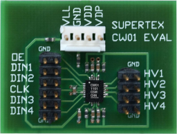
The CW01 has 6 logic inputs; OE, CLK, DIN1, DIN2, DIN3, and DIN4. Every logic input has a 10kΩ pull down resistor. There are 3 power input voltages: VLL, VDD and VDX. VLL is the input logic level, typically 2.5V. VDD is the level translator, typically 5.0V. VDX is the gate drive voltage, and is at the same voltage level as VDD. High peak currents will be drawn from VDX during switching. Each supply has a series ferrite bead and a 0.1μF ceramic chip capacitor to keep the supply clean from high frequency noise. There are 4 outputs: HV1, HV2, HV3 and HV4. These are the connections to the drains of 100V, 7.0Ω, N-channel MOSFETs.
Please download the user guide for more information
Cannot load image!
Documentation
Filter by Document Type
Search Documentation
|
Title
|
Document Category
|
|||
|---|---|---|---|---|
| CW01DB1 Demonstration Board User Guide | User Guides | Download |