Log in to myMicrochip to access tools and benefits. Sign up in just one minute.
Maximize Your Experience: Reap the Personalized Advantages by Completing Your Profile to Its Fullest. Update Here
Stay in the loop with the latest from Microchip. Update your profile while you are at it. Update Here
Complete your profile to access more resources. Update Here
Overview
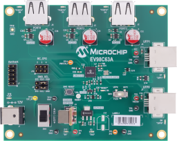
The EVB-USB2534D is an evaluation and demonstration platform featuring the USB2534 USB 2.0 hub on a 4-layer RoHS compliant Printed Circuit Board (PCB). It is designed to demonstrate the unique features of this device using a low-cost PCB implementation with individual port power control for the downstream USB 2.0 ports. All downstream USB 2.0 ports include a high current port power controller to fully support USB battery charging as a high current walk-up port.
- 36-pin QFN RoHS compliant package
- Four USB 2.0 downstream hub ports with individual port power and overcurrent sense (OCS)
- High-Speed (480 Mbps), Full-Speed (12 Mbps) and Low-Speed (1.5 Mbps) compatible
- USB Battery Charging is supported on all downstream USB ports up to 2A
- Multi-Transaction Translator (MTT) is enabled
- Supports internal default hub configuration. Optionally supports configuration from external EEPROM
- Low-Cost, 4-Layer space saving design with two outer signal layers, a power inner layer and a ground inner layer
- Individual port power control with LEDs for port power indication
- Self-Powered operation
- Operates from a single voltage (12.0 VDC, regulated) external power supply
- External supply provides up to 6A of 5.0 VDC for system use and USB downstream power through an on board 5 VDC regulator
- On board MCP1725 3.3 VDC regulator provides power to the USB2534 circuits and RESETn control
- LED indicator for “Suspend” hub state (optional)
- EMI suppression provided by selection of capacitors and inner power/ground Printed Circuit Board (PCB) layers
- ESD component footprints provided (optional)
- Single crystal clock source
- Schematics, layout and bill of materials are available to minimize new product development time
Cannot load image!