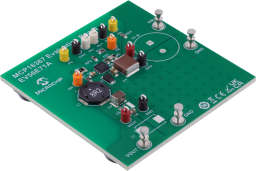
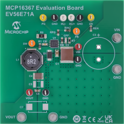
Overview
The MCP16367/8/9 family of devices are highly integrated, high-efficiency, fixed-frequency, step-down DC-DC converters in a compact 8-lead 3x3 mm VDFN package that operates from input voltage sources up to 48V. Integrated features include a high-side switch, fixed-frequency Peak Current Mode Control, Internal Compensation, Power Good, Peak Current Limit and Overtemperature Protection. The MCP16367/8/9 can regulate the output voltage over a wide 2V to 20V range, and typically can deliver over 400 mA of load current at 3.3V output, when supplied from a 12V input. The maximum input voltage range is 4V (after Start-up) to 48V. The regulated voltage (VOUT) should be lower than the input voltage (VIN).
• Input Voltage Range (VIN): 4.0V (after Start-up) to 48V
• Output Voltage: 3.3V
• Output current: 400 mA @ 3.3V Output (typical), 12V Input
• Automatic PFM/PWM Operation for MCP16367
• PWM Switching Frequency: 2.2 MHz
• Low Device Shutdown Current: 3 μA, typical
• Low Device Quiescent Current: 18 μA, typical (not switching)
• Integrated N-Channel Buck Switch ON State Resistance: 500 mΩ
• Internal Compensation
• Internal Soft-Start
• Internal Bootstrap Diode
• Internal Current Limit
• Power Good Output
• Overtemperature Protection (if the die temperature exceeds +155°C, with 25°C hysteresis)


Documentation
|
Title
|
Document Category
|
|||
|---|---|---|---|---|
| EV56E71A_BOM | Board Design Files | Download | ||
| EV56E71A_SCH | Board Design Files | Download | ||
| EV56E71A_GERBER | Board Design Files | Download | ||
| EV56E71A_China-RoHS-Declaration | Certifications | Download | ||
| EV56E71A_EU-REACH-Statement | Certifications | Download | ||
| EV56E71A_EU-DoC | Certifications | Download | ||
| EV56E71A_UK-DoC | Certifications | Download | ||
| EV56E71A_Design_Files.zip | Board Design Files | Download | ||
| MCP16367 Evaluation Board User’s Guide | User Guide | Download |