Mastering Timing Analysis and Debug Using Libero® SoC Design Suite
Get a practical overview of timing analysis using SmartTime in our Libero® SoC Design Suite. This post highlights problem areas and guides practical fixes, and explains why timing matters, how common issues arise and how SmartTime helps designers validate performance before hardware deployment.

Microchip Field-Programmable Gate Arrays (FPGAs) are designed for a wide range of applications including embedded systems, communications, defense, automotive and industrial control. These FPGAs are known for their low power consumption, high reliability and robust security features. In addition, we provide a set of design tools to develop FPGA-based hardware systems.

Figure 1 - Power-Efficient Mid-Range FPGAs and SoCs With the Highest Reliability and Best-in-Class Security
Designers have been challenged with defining and verifying timing related issues for many years. These issues can arise from many causes like missing, malformed or competing constraints within the hardware design. To make it easy to define and verify timing issues, we have developed Libero® SoC Design Suite to provide all the necessary tools to developers to accelerate their designs.
It is essential to not only enter constraints but also verify timing performance of a design and ensure it meets specified clock frequencies. This static timing analysis identifies potential timing violations (setup/hold issues) before device programming, saving significant time to market.
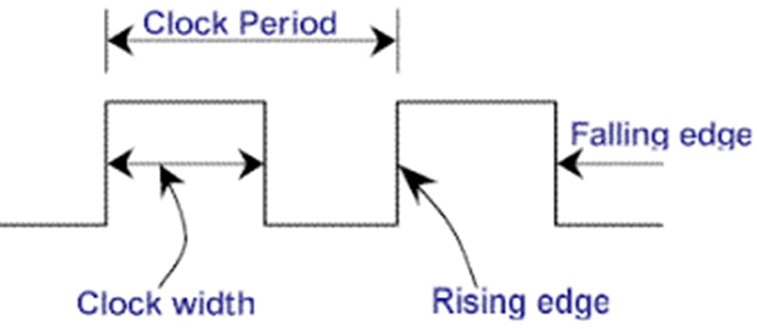 |
Figure 2 - Clock Definition
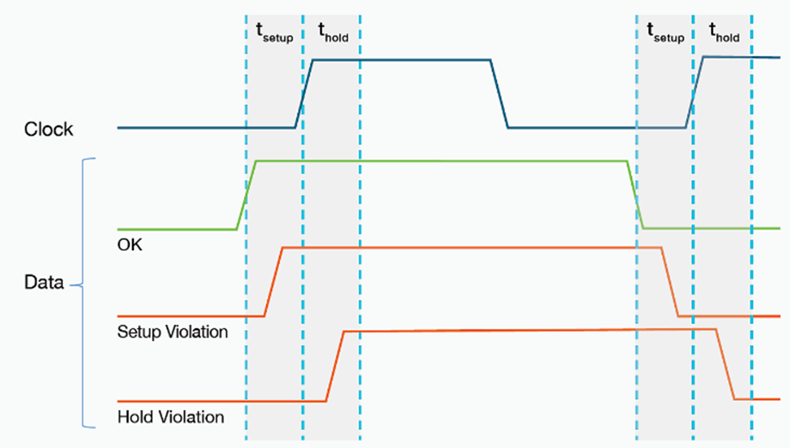 |
Figure 3 – Clocks Setup and Hold Timing
Developers will not only define and verify constraints but also need to debug timing related issues that arise from issues with constraints quickly and efficiently.
Design Guidelines
Any developer creating Microchip FPGA-based hardware should follow a set of guidelines for various stages of development.
Design Phase
It is important to align user-defined RTL with FPGA device architecture for optimizing performance. This includes understanding the device architecture and an efficient plan for utilizing the device’s hard IPs and I/O pin layout. In addition, a designer should follow custom or user-defined coding guidelines to make verification and debug easier. The use of synchronous design methodologies, pipelining for timing, properly designed cross clock and reset domains and adding registers to hard block I/O should help address common issues.
Applying Constraints
While applying design constraints, designers should derive the general constraints for the IP core components in the overall design and create constraint files for user-defined clocks. These constraints are used for Synthesis, Place and Route (P&R) and timing verification. The Libero Constraints Manager tool enables deriving and defining various constraints and timing exceptions.
Synthesis
After synthesis, a timing report is generated, and it indicates timing goals not met; the designer can enable retiming and adjust RAMs for high-speed which may address these issues. Also, make sure to look at all critical paths in reports, declare the clock groups and their relationships, minimize logic levels, reduce high-fanout nets and verify global routing.
Place and Route
If the post-P&R timing reports have issues, the designer should work towards classifying and understanding the violations. After understanding the violations, the designer can formulate a plan for addressing each type of violation. Gross violations might require design changes at the RTL and block level.
Libero provides P&R options, such as driver replication, high effort layout and repairing minimum delay violations as well as multiple passes to help address smaller timing issues; these options may increase runtime but could provide better timing.
The Constraints Manager makes it easy to separate the timing constraints applied during Synthesis and Layout versus those applied for Static Timing Analysis (STA). This enables the designer to over-constrain key paths or domains in the timing constraints used for Synthesis and Layout, to reduce timing violations against the actual constraints used for STA. Also, consider using placement constraints and I/O register combing.
Libero SoC Design Suite
Libero is an integrated development environment (IDE) used for designing and implementing hardware systems targeting our FPGA families. This includes a complete hardware flow from RTL entry to bitstream generation and specific tools for defining, verifying and debugging constraints and timing issues.
- Constraints Manager: Organize constraints used for which tool flow step and editor allows designer to create/edit design timing and placement constraints
- DRCs: Automated design rule checking
- Chip Planner: Allows designers to view physical layout and routing of design
- Simulation: Functional and timing verification
- SmartTime: Performs STA and report timing issues
Constraints Manager
The Constraints Manager provides a single view to manage all these constraint files, and their association to synthesis, place-and-route, and timing verification which generally fall into three categories.
- Timing Constraints (SDC): Defined using the industry-standard format, and includes clock definitions and attributes, I/O delays and timing exceptions, such as false and multi-cycle paths
- Physical Design Constraints (PDC): Specify I/O pin assignment and attributes, as well as physical placement through floor planning
- Synthesis Constraints (FDC): Synthesis specific and can include preserving specific hierarchical names or forcing certain logic implementations
Libero’s Constraints Manager enables designers to meet performance goals by providing a structured path for entering performance requirements, guiding tool prioritization, simplifying constraint management, providing design reproducibility and automating constraint generation.
Design Rule Checks (DRCs)
A constraint DRC is a check that ensures your constraints are valid, consistent and correctly applied to your design. These help to verify the tool rules not logic itself and are critical because applying incorrect constraints is as bad as no constraints at all. Some of the common errors include syntax, logical errors and incomplete/inconsistent constraints.
The constraints manager doesn't have a single, unified "DRC" function, but rather a set of features that help you perform these checks and establish your constraints are correct. The DRCs are run when entering/importing constraints, verifying constraint coverage, deriving constraints and cross probing with SmartTime and Chip Planner.
On top of the DRCs available in the Constraints Manager, the Libero SoC design implementation flow performs device and design specific DRCs on the user constraints. Starting with the Synthesis tool, a constraint check report is generated in the project’s Synthesis subfolder, to identify issues with the user timing constraints. Later, during Compile and Place and Route, the validity of I/O assignments, global signal assignments, floor planning constraints and timing constraints is checked for validity. Issues are reported in the Log and Message windows, and the referenced report files, along with specific design elements in question and potential reasons, if available.
SmartTime
A static timing analysis tool is used within the Microchip Libero SoC design suite and is a critical part of the design flow. This allows designers to verify that digital circuits operate at the desired speed and correctly.
- STA checks all design timing paths without simulating every input combination, for fast and efficient timing violation investigations
- Timing Constraints are provided to SmartTime using timing constraints file, that specifies clock frequency, clock attributes, I/O delays and timing exceptions
- Timing Violation Reporting checks the design using specified constraints, then generates timing violation reports to identify setup/hold time violations and clock domain issues, across multiple device operating corners
- Post-Layout Verification using SmartTime by analyzing the physical design layout accounting for actual wire and cell delays
- Cross-Probing allows designers to select a timing path or component in SmartTime and visualize its physical location and connections for easier debugging
Designers can use it to verify that a digital design meets all its timing requirements across various operating conditions like timing margins across process, voltage and temperature (PVT) variations. In addition to verifying timing, it can help debug problems arising from timing within FPGA designs.
- Displays detailed timing paths and filtering for focused analysis
- Shows results of applied constraints
- Reports: Expanded path, positive/negative slack, others
- Identifies potential metastability issues between asynchronous clock domains
- Detects and reports logic loops that can cause unpredictable behavior
Debug Timing Violations in SmartTime
Debugging timing violations in Microchip's Libero SmartTime is a crucial part of the FPGA design flow to ensure your circuit functions correctly at the desired speed. It's an iterative process that involves identifying the violation, understanding its cause and then taking steps to fix it.
Analyze the SmartTime Reports
First, open SmartTime and examine reports, with the most important being the Timing Violations Report. This report will list all paths that have a negative slack, which is your primary indicator of a timing failure.
- Slack: Shows slack for each violating path, for a failing path a negative slack value will exist
- Source and Destination: Identifies start and end points of violating path, which are usually flip-flops or I/O ports
- Path Details: Breakdown of path, including delays from clock network, logic cells and routing wires
Nature of Violation
Setup and Hold violations are the two main types of timing violations encountered. Setup violation is when data takes too long to travel from the source flip-flop to the destination flip-flop. This is the most common type of violation and is usually related to the clock frequency being too high or the logic between the flip-flops being too complex.
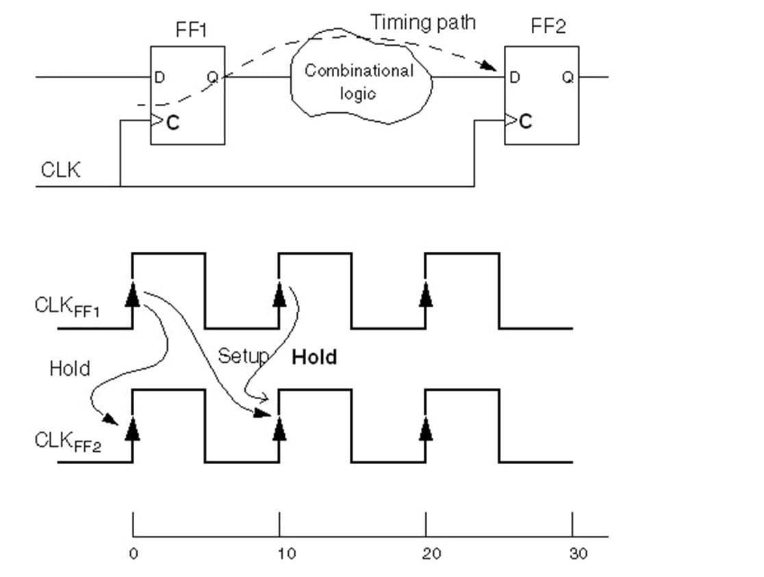 |
Figure 4 - Setup/Hold Timing Violation
The second and least common is a hold violation which means the data arrives too quickly at the destination flip-flop and changes before the required hold time has passed. This can be caused by very fast paths with little logic and a significant clock skew.
Cross-Probing
SmartTime integrates with other tools in Libero like Chip Planner, which has some very powerful debug features like visualizing the path, identifying congestion and locating logic. Selecting a violating path in SmartTime report design can choose to "cross-probe" to the Chip Planner, which will highlight the physical location of cells and the routing resources. If a path crosses a large portion of the chip or goes through a very congested area, it's a strong indication that routing delays are the problem. The logic cells in path can be seen, identifying the complex block of logic which is causing a long combinatorial delay.
Selecting a net of interest also provides properties such as the fanout, as well as a visual representation of all the destination cells, if enabled in the display settings. These tools can help identify situations where the cell placement and net delays are due to high utilization of physically bound device resources, such as fabric RAM blocks. These tools enable deeper understanding of the violation and potential reasons so the user can formulate a strategy towards resolution.
Fix Timing Violations
Once you've identified the cause of the violation, the best approach depends on the nature of the problem. If the violation is due to a long combinatorial path, then pipelining, logic optimization or using timing-driven place and route could help. Pipelining will help to break up the long path by inserting new flip-flops which will add a clock cycle of latency but shortens the path delay.
Logic optimization can simplify the logic and the associated path. With appropriate timing constraints from the user, the default timing driven P&R prioritizes meeting timing constraints during the physical implementation and for small setup violations, we can also try increasing the "effort level" of the Place and Route tool.
As another example, the user can employ synthesis directives to steer the design implementation, such as replacing a high number of inferred cascaded small RAM blocks (uSRAMs) with much fewer large RAM blocks (LSRAMs), to reduce the physical span required for RAM control signals, potentially optimizing the placement and reducing the arrival time path delay.
However, if the violation is a hold violation, then we can focus on the place and route settings and potentially add buffers. The “Repair min delay violations" can automatically insert small buffers on fast paths to add delay and fix hold issues. Since this may not be enough a design may need to manually add buffers on paths that are failing hold time.
Typically, the initial place and route should be performed without minimum delay repair (MDR) enabled, so the user can understand and categorize the hold violations, before applying a resolution strategy. Sometimes it might only require buffers to delay the data path slightly or require adding programmable input delay for source synchronous inputs, while other times might require additional logic to prevent the violation.
Iterative Process
Debugging timing violations is not a one-and-done process. You will likely go through several iterations which include identifying the violation hypothesize on cause, modifying code, constraints or place and route settings. Once that is completed with updates in place, re-run synthesis and Place and Route steps and re-analyze timing reports. By following this systematic approach, designers effectively use SmartTime to diagnose and fix timing issues and meet performance goals. A general guideline is to fix the large timing violations first, since those often require changes to the design RTL or architecture. Once max delay timing is closed and gross hold time issues are addressed, smaller min delay violations can be addressed using Incremental place and route, with minimum delay repair enabled.
Example Design and Constraints for Libero
Here’s a complete example of a carry-over counter design for Microchip FPGAs using Libero SoC, which includes the design and constraints.
module carry_counter (
input wire clk, input wire rst_n,
output reg [3:0] count, output reg carry
);
always @(posedge clk or negedge rst_n) begin
if (!rst_n) begin
count <= 4'b0000;
carry <= 1'b0;
end else begin
if (count == 4'b1111) begin
count <= 4'b0000;
carry <= 1'b1;
end else begin
count <= count + 1;
carry <= 1'b0;
end
end
end
endmodule
Libero integrates support for various timing constraints for timing (SDC), as shown in the example.
Constraint | Description |
create_clock | Defines a primary clock signal, its period, and waveform. |
create_generated_clock | Defines a derived clock from a base or reference clock (e.g., PLL output) |
set_input_delay | Specifies delay from external input to design relative to a clock. |
set_output_delay | Specifies delay from the design to an external output relative to a clock. |
set_clock_groups | Organizes clocks into groups and specifies the relationship between those groups |
set_false_path | Ignores specific paths during timing analysis. |
set_multicycle_path | Specifies paths that take multiple clock cycles. |
set_max_delay / set_min_delay | Sets custom delay constraints between points. |
set_clock_uncertainty | Adds margin to account for clock jitter or skew. |
set_disable_timing | Disables timing analysis on specific paths or cells. |
At a top level, the designer will need to define at least one clock with constraints, and the following is an example of how to complete that effort.
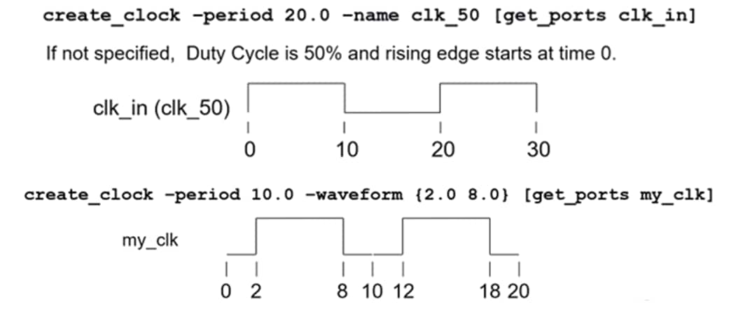 |
Figure 5 - Example Clock Creation with 50% and Defined Duty Cycle
Using these constraints within the SDC files that are generated by the constraints editor or manually imported, the constraints to define the design example to run at 200MHz with input/output delays are shown below.
# Define 200 MHz clock (5 ns period)
create_clock -name clk -period 5.000 [get_ports clk]
# Input delay (assuming external device drives input)
set_input_delay -max 2.5 -clock clk [get_ports rst]
# Output delay (assuming external device captures output)
set_output_delay -max 2.5 -clock clk [get_ports count]
set_output_delay -max 2.5 -clock clk [get_ports carry]
To attach the I/O to physical pins, the designer will need to utilize the Physical Design Constraints (.PDC file). As a quick example, these are common options provided for designers within Libero to define constraints.
Commands | Description |
set_io | Assigns I/O standards, voltage levels, and drive strength to pins |
set_iobank | Sets the input/output supply voltage (vcci) and the input reference voltage (vref) for specified I/O bank |
set_location | Fixes a logic element or I/O to a specific physical location, if performing manual floor planning. |
set_region | Constrains logic to a specific region of the FPGA fabric, when performing manual floor planning. |
define_region | Creates a named region for use in set_region |
set_ioff | Specifies whether or not a register is combined with I/O during Synthesis |
set_preserve | Compile will preserve these instances and not combine them. |
assign_region | Constrains a set of macros to a specified region |
assign_net_macros | Assigns all macros connected to a net to a user-defined region |
define_region | Defines a rectangular region or a rectilinear region |
move_region | Moves named region to specified coordinates |
edit_io | Make changes related to GPIO and HSIO type I/Os |
edit_instance_delay | modify the instance delay properties |
Example uses of these commands are provided in the Microchip Libero documentation and can help designers set up the physical design constraints quickly. Using the I/O Attribute Editor makes the job of making assignments much easier and can provide a simple example to follow when editing manually.
Common FPGA Constraint Issues and Libero Solutions
Designers frequently run into several constraint-related issues during FPGA development, and the following steps help identify and resolve them using Libero tools and TCL commands. In the initial stages of design, focus should be applied to the following quick start steps to address issues.
- Synthesis and RTL changes have the biggest impact
- Review Synthesis reports and pipeline deep combinatorial paths to reduce the number of logic levels
- Review CDC paths and design proper clock domain crossing and reset domain crossing logic
- Understand logic mapping (FSM encoding) and hard-IP block utilization details to find potential optimizations
- Pipeline MATH and RAM blocks to improve performance, do not have in critical path
- Place and route effort
- Use regular P&R effort (close to final performance ~3-5%), better runtime
- In final design phases change to high effort if needed
- Run min/max delay STA
- Early: Do not run min-delay repair, typically small QoR change and longer runtime. Focus on max-delay timing closure
- Late: Enable min-delay repair with incremental P&R to resolve hold violations while retaining max-delay timing closure
- Multi-pass place and route
- Early: Don’t run multi-pass P&R, make RTL/synthesis changes 1st to get QoR margin
- Late: Run multi-pass (i.e. 5 passes) place and route, combined with high-effort, if necessary to potentially squeeze out a bit more timing margin (up to ~5%).
- Reduce physical location constraints number, especially ones added for timing closure
- Use wildcards in constraints only when necessary, as they can expand into many unnecessary constraints and affect QoR and runtime.
In addition to these quick steps, the following are steps provided to address specific issues.
Incomplete or Missing Clock Constraints
This is the most fundamental and frequent error—without proper clock definitions, Libero's timing engine (SmartTime) cannot accurately analyze your design's performance, leading to unpredictable hardware behavior.
- Issue: Synthesis and place and route tools don't know the target frequency of your clocks, making timing analysis meaningless
- Designers must set the clock constraint
- create_clock -name {my_system_clk} -period {10.0} [get_ports {clk_i}]
- create_clock: Defines a primary clock.
- -name {my_system_clk}: Assigns a unique name to the clock
- -period {10.0}: Specifies clock period in nanoseconds
- [get_ports {clk_i}]: Identifies the clock pin connected to the FPGA input port named clk_i
- To debug these types of errors within Libero verify timing using SmartTime.
- Look and see If clock isn't listed or shows an "unconstrained" in SmartTime
- Review the constraints coverage report
- Potentially large negative slack violations if clocks aren't defined
Incorrect or Overly Optimistic Clock Frequencies
Setting an unreachable clock frequency for the Verify Timing SDC constraints used for STA can lead to persistent timing violations and prolonged debugging. This does not refer to using an over-constrained clock period for Synthesis and P&R, in a separate SDC versus Verify Timing SDC.
- Issue: Target clock period is too aggressive for design or the target device
- Designers should adjust the create_clock period
- # Gradually increase period (decrease frequency) until timing closed
- create_clock -name {my_system_clk} -period {15.0} [get_ports {clk_i}]
- Debug this error within Libero by analyzing the Setup Slack report
- Negative slack on many paths even after optimization attempts, your clock frequency might be too high
- Look for negative slack paths in SmartTime to identify slow logic for target frequency
Missing Input/Output (I/O) Constraints
Failing to constrain I/O delays prevents accurately verifying the timing interaction between FPGA and external components.
- Issue: FPGA works internally, but communication with off-chip devices (e.g., ADCs, DDR memory) fails due to setup/hold violations at the I/O pins
- Make sure the design has the correct design constraints set
- # For an input signal 'data_in' clocked by 'my_system_clk'
- set_input_delay -clock {my_system_clk} -max {2.0} [get_ports {data_in}]
- set_input_delay -clock {my_system_clk} -min {1.0} [get_ports {data_in}]
- # For an output signal 'data_out' clocked by 'my_system_clk'
- set_output_delay -clock {my_system_clk} -max {3.0} [get_ports {data_out}]
- set_output_delay -clock {my_system_clk} -min {0.5} [get_ports {data_out}]
- # -max/-min: Define the worst-case and best-case delays. These values # come from external component datasheets and board trace delays.
- To debug look for setup/hold violations and make sure the I/O are registered for timing critical I/O
Incorrect I/O Standards or Drive Strengths
Improper I/O configurations can lead to signal integrity issues, data corruption or even device damage.
- Issue: External communication fails due to voltage mismatches, insufficient drive current or poor signal quality.
- Define I/O technology and configure parameters for I/O placement
set_io -port {data_in_port} -std {LVCMOS18} -schmitt_trigger {ON}
set_io -port {data_out_port} -std {LVCMOS25} -slew {FAST} -current {8}
- Inside Libero verify that the set_io commands have been successfully applied and are compatible with the selected device and/or pin. Designers can also use a scope to check signal integrity, voltage levels and rise/fall times.
Unnecessary or Incorrect Timing Exceptions
Misusing set_false_path or set_multicycle_path can mask real timing issues or introduce new ones. The set_clock_groups command can be used to define the relationship between different clock domains which helps to avoid false timing paths, improve accuracy, optimize tools and support multi-clock designs. Three of the common clock group relationships are listed below.
- Asynchronous: No timing relationship; paths between domains are ignored
- Exclusive: Only one clock is active at a time; no timing paths between them
- Related: Clocks have a known phase/frequency relationship; timing paths are analyzed
This command is powerful and critical to guide the STA engine to correctly analyze or ignore specific timing paths. Use these on asynchronous clocks which are derived from different, unrelated clocks sources (e.g., clock from external oscillator and a fabric-based clock from a separate clock input). Not declaring these clocks asynchronous will cause SmartTime to try and perform a synchronous timing analysis between them, leading to incorrect timing reports or overly conservative design.
- Issue: Critical path is erroneously ignored, or a path is given too many cycles when it could achieve single-cycle performance
- Libero provides a constraint to define an asynch reset
- # Correctly identify asynchronous reset path as false
- set_false_path -from [get_ports {async_reset_n}]
- # Allow a path between two modules to take 2 clock cycles
- set_multicycle_path -setup 2 -from [get_pins {moduleA_inst/q_reg}] -to [get_pins {moduleB_inst/d_in}]
- set_multicycle_path -hold 1 -from [get_pins {moduleA_inst/q_reg}] -to [get_pins {moduleB_inst/d_in}]
- Debugging within SmartTime in Libero by verifying that only intended paths are false-pathed or multi-cycled. Also be aware, the ultimate test for timing exceptions is back-annotated post-layout timing simulation with design-specific SDF, which might reveal functional errors even if STA timing passes.
Clock Domain Crossing (CDC) Issues
CDC paths need careful synchronization and specific constraint handling to prevent metastability and functional errors.
- Issue: Signal(s) crossing between unsynchronized clock domains are prone to metastability, leading to unpredictable system behavior. So, design proper CDC synchronizers (e.g., two-flop synchronizer, asynchronous FIFOs for data, synchronize the release of async resets)
- Setting constraints is vital (after synchronizer), for a correct and reliable design because STA needs explicit instructions on how to handle
- # Assuming 'data_async_out_s1' is the output of the first flop in a 2-flop synchronizer
- set_false_path -from [get_pins {*data_async_out_s1}] -to [get_pins {*data_async_out_s2/D}]
- Libero has basic CDC analysis features to report potential metastability issues or unsynchronized crossings designed to improve reliability and performance. Turn on the option for automatically detecting CDC synchronizer circuits, safe CDC and forward annotation of netlist to drive the place and route correctly. To find these issues, look for specific warnings from the synthesis or timing tools regarding unconstrained or unsynchronized CDC paths. Also simulate with gate-level or post-P&R delays as it can sometimes reveal metastability issues, though it's not foolproof. However, the complete solution is to utilize a commercially available CDC analysis tool.
Missing/Poor PDC
Plan the design architecture and pin assignment in a manner that accounts for the physical location of device-specific hard IP blocks, to ease the job of the Place and Route tool. For example, model the data flow of the design by overlaying the physical location of hard IP blocks in the device to ensure I/O pin selection, transceiver block selection and even device orientation on the board is optimal to promote efficient P&R results within the device. A poorly planned top-level pin assignment and hard-IP block selection can result in sub-optimal P&R results. In some scenarios, without user floor-planning guidance, the placer might distribute critical logic widely, leading to long routing delays and timing violations.
- Issue: It is possible for place and route to make a poor placement decision leading to timing issues
- For this make sure to create regions for critical modules.
- # Create a rectangular region for a critical module
- create_region -name {DSP_CORE_REGION} -type {RECT} -pnt1 {R5C5} -pnt2 {R10C10}
- # Assign the critical instance 'my_dsp_top_inst' to this region
- set_location -region {DSP_CORE_REGION} [get_instances {my_dsp_top_inst}]
- # Assign a specific I/O port to a physical pin
- set_location -pin {P10} [get_ports {debug_led_o}]
- To debug in Libero, complete flow through place and route, then open the Chip Planner and visually inspect where your critical modules are placed. Also, check PDC Report for warnings or errors (e.g., "Region Overlap," "Instance not placed in region")
Make sure to verify that there are no placement constraints conflicting with fixed locations of hard IP within FPGA (e.g. DDR, MATH, RAM, transceivers, etc.). Consider whether many cascaded uSRAMs can be replaced by a single LSRAM, to reduce the span of RAM block control signals across the FPGA fabric.
Conclusion
Microchip's Libero SoC Design Suite is an essential and comprehensive set of tools for developing FPGA-based systems. A key aspect of this process is mastering timing and debugging, which is achieved through a systematic approach. This involves not only correctly defining a wide range of constraints (timing, physical and synthesis) but also using sophisticated tools like SmartTime for static timing analysis and Chip Planner for physical layout visualization.
Effective debugging is an iterative process of identifying timing violations (setup/hold), understanding their root cause and then applying appropriate fixes such as pipelining, logic optimization or adjusting place and route settings. By following a structured methodology and using Libero's integrated features, designers can be confident that their FPGA designs meet all performance goals and function reliably.