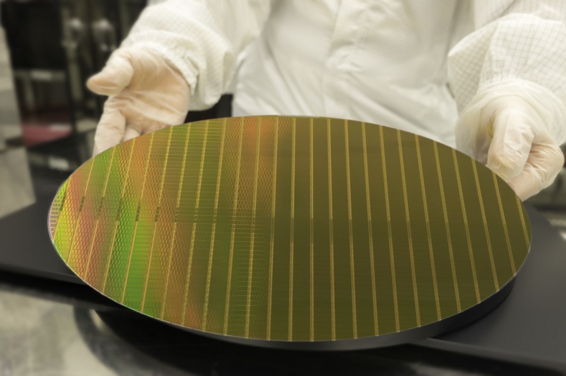
Wafer Foundry Services
Live Chat
Need Help?
Privacy PolicyCustomized Wafer Foundry Solutions
Advanced Technologies for Your Custom Projects
We offer core competencies in the following areas:
- CMOS
- Bipolar-CMOS-DMOS (BCD)
- Embedded Nonvolatile Memory (eNVM)
- Interposer
- Silicon-on-Insulator (SOI) high-voltage technologies
- Charge Coupled Devices (CCDs)
- Micro-Electrical Mechanical Systems (MEMS)
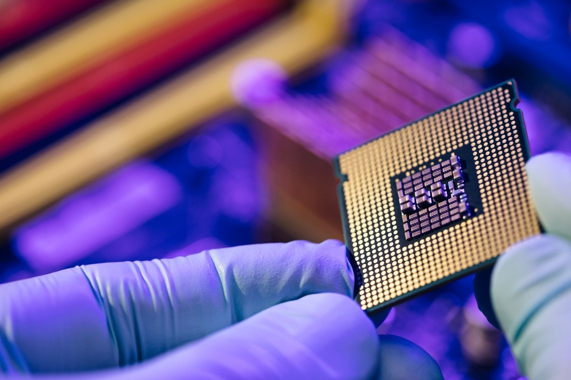
Custom and Standard Process Services

Full and Semi-Custom Processes
- Transfer your existing process from another fab or university
- Create a custom process using our vast catalog of standard process modules
CCDs
- Standard process flows available at various nodes that can be tailored to your specifications
- I-line lithography with stitching option available for large sensors
MEMS
- Thin wafer handling
- Specialized equipment including DRIE, backside processing with frontside alignment, wafer bonder, 1X aligner, KOH etch and CPD
Unit Processes
- Epitaxial silicon growth
- Ion implant
- Species available: B, P, As, Sb
- Wide range of doses and energies available
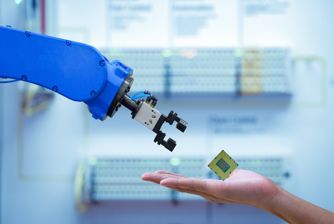
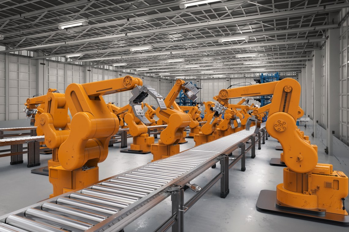
Manufacturing Capabilities: Speed, Precision and Quality
We combine advanced manufacturing systems with a global network of facilities to ensure high-quality production with exceptional efficiency. Our factories, located in the U.S., Europe and Asia, allow us to shorten cycle times and deliver products quickly, meeting the demands of customers around the world. Whether we're handling large orders or smaller, specialized batches, we maintain consistent product quality with automated processes in place. This flexibility helps us scale production to meet varying customer needs while ensuring precision.
By controlling every aspect of production from wafer fabrication to final testing, we can deliver reliable, high-performance products every time and uphold the highest industry standards. Our commitment to speed, quality and precision makes us a trusted partner in meeting your manufacturing needs.
Trusted Quality and Certifications
We are committed to delivering high-quality products and services. Our wafer fabrication and assembly/test facilities are certified to ensure we meet the highest industry standards. These certifications help guarantee the reliability and excellence of our products.
Key Certifications:
- ISO 9001: Ensures quality management and consistent products
- IATF 16949: Meets automotive industry standards for quality
- AS9100: Certified for aerospace and defense industry standards
- DLA 19500 & 38534: Ensures military-grade reliability and performance
- MIL-PRF-19500 (JANS): High-reliability certification for military applications
- MIL-PRF-38534 (H/K): Ensures top quality for space and defense applications
These certifications demonstrate our dedication to providing you with trusted, reliable products.
Microchip Expands TSMC Partnership for Enhanced Manufacturing
We have expanded our partnership with TSMC to boost 40 nm manufacturing at Japan Advanced Semiconductor Manufacturing (JASM) in Kumamoto. This collaboration enhances our supply chain resiliency and meets growing demand across automotive, industrial, and networking sectors, strengthening our ability to serve our customers.
Contact Us
To learn how our wafer foundry services can meet your specific requirements, reach out to our Foundry Team.