We detect you are using an unsupported browser. For the best experience, please visit the site using Chrome, Firefox, Safari, or Edge. X
Maximize Your Experience: Reap the Personalized Advantages by Completing Your Profile to Its Fullest. Update Here
Stay in the loop with the latest from Microchip. Update your profile while you are at it. Update Here
Complete your profile to access more resources. Update Here

FPGA Design Services and Check

Live Chat

Need Help?

Privacy Policy

Design Services


Our FPGA design services leverage a world-class team of design experts to expedite your design cycle with guaranteed quality. We tailor our expert services to key vertical and horizontal solutions for Machine Learning (ML), Smart Embedded Vision (SEV), high-speed communications and motor control. Design offerings include a broad range of design items such as new module and IP development, IP customization, design optimization, fitting and system development.

Leverage our:      

  • FPGA/SoC experts: a team of experts with experience with our FPGAs and popular industry-standard development tools
  • Proven design capabilities: extensive application experience with FPGA/SoC model-based designs, HDL IP and firmware development
  • Dependable quality and reliability: certified quality management process
  • Robust risk management process: structured, transparent and continually reassessed process with a dedicated program manager

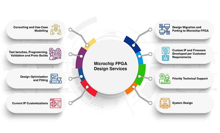
Reduce Risks and Costs and Fast-Track Your FPGA Design in Three Easy Steps


  1. Talk to us to help us understand your design requirements. 
  2. Work with us to craft and sign a Statement of Work (SoW).
  3. Perform periodic reviews as we develop and test your design.

Our Solutions


FPGA Design Services Video

Watch this short video to get an overview of our FPGA design services.

Design Check


Reduce design risk and accelerate your FPGA development with our expert design review services.

Our specialists analyze your schematics and PCB layout to identify issues early by focusing on DDR, SerDes signal and power integrity, where failures are most likely.

Get a clear, actionable report with:

  • Key risk areas
  • Targeted recommendations
  • Performance optimization insights

Move faster, avoid re-spins and improve first-pass success.

Explore the service levels below to get started.

DescriptionCharges and
Turnaround Time
Input RequiredItems Covered and Delivery Format
FPGA Design Check (L1)—Board Design GuidelinesFreeN/ABasic checklist based on the board design guidelines—case/email communication on the portal

FPGA Design Check (L2)—Schematics Only

3,000 USD

(5 days)

Schematics

Detailed review report with recommendations for:

  • Board guideline check
  • Libero® PDC validation
  • IO and SerDes assignment
  • Clock/reset review
  • Power recommendations
FPGA Design Check (L3)—Layout Review

5,000 USD

(6 days)

Layout file
(.brd or ODB++ format)
Document report with layout feedback
FPGA Design Check (L4)—Signal IntegrityDDR Simulations
10,000 USD
(10 days)


  • Schematics
  • Layout file ( .brd or OBD++ format)
  • Board stack-up details
  • Additional questions, if any 
Document report with standard simulation results 
SerDes
12,000 USD
(10 days)
Document report with setup details, modeling, cutout recommendations
FPGA Design Check (L5)—Power IntegrityPower Integrity 
Simulation

15,000 USD
(15 days)
Document report with simulation results and
optimization recommendations
FPGA Design Check (L6)—Bundle Service30,000 USD
Discounted price for all
services combined
         All of the aboveAll of the above

Live Chat

Need Help?

Privacy Policy